In the world of electronics, converters play a pivotal role in transforming electrical energy from one form to another. Whether it’s converting AC to DC, stepping up or down voltage levels, or changing the frequency of a signal, converters are essential building blocks in numerous applications. However, these converters are not without their challenges. Parasitic components, unwanted elements present in converter circuits, can significantly impact their performance and efficiency. In this blog post, we will delve into the realm of parasitic components, exploring their origins, effects and mitigation techniques in the context of converters.
The Nature of Parasitic Components
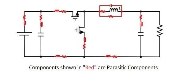
Parasitic components refer to unintended elements in a circuit that arise due to the inherent properties of components, interconnections, and their interaction with the environment. These components are typically unwanted and can manifest in various forms, including resistance, capacitance, inductance and leakage elements. Understanding and mitigating the effects of these parasitic components is crucial to achieving optimal performance in converter circuits.
The Impact of Parasitic Components
Parasitic components can have a range of detrimental effects on converters, including:
a. Losses and inefficiency: Parasitic resistances in components and interconnections lead to power dissipation and reduced efficiency in converters. These losses can cause heating and limit the overall performance and reliability of the system.
b. Transient response issues: Parasitic capacitances and inductances can affect the transient response of converters, leading to voltage spikes, ringing, or overshoots. These undesirable behaviors can impact the stability and reliability of the circuit.
c. EMI/EMC concerns: Parasitic elements can contribute to electromagnetic interference (EMI) and electromagnetic compatibility (EMC) issues in converter circuits. Unwanted electromagnetic emissions can interfere with other nearby components or systems, causing performance degradation or malfunction.
d. Timing and synchronization challenges: Parasitic elements can introduce delays or distortions in signals, affecting the timing and synchronization of converter operations. This can lead to errors, reduced accuracy or even circuit failure.
Identifying Parasitic Components
To address the issues posed by parasitic components, it is essential to identify their presence and quantify their impact. Several techniques can help in identifying and characterizing parasitic elements, including:
a. Circuit analysis and simulation: Circuit analysis tools, such as SPICE simulations, enable designers to predict the behavior of converters and estimate the impact of parasitic components. These tools provide insights into voltage drops, current flows and other performance parameters.
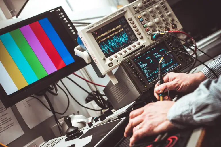
b. Measurement and characterization: Using specialized instruments like oscilloscopes, network analyzers, and impedance analyzers, engineers can measure and characterize the parasitic components in a converter circuit. These measurements help in validating the simulation results and refining the design.
c. Component datasheets and models: Manufacturers often provide datasheets and models that include parasitic information for their components. These resources can serve as a starting point for understanding and accounting for parasitic effects in the converter design.
Mitigation Techniques
To mitigate the adverse effects of parasitic components, several strategies can be employed:
a. Component selection: Choosing components with lower parasitic characteristics, such as low equivalent series resistance (ESR) capacitors or low series resistance inductors, can minimize their impact on the converter’s performance.
b. Layout and routing: Optimizing the layout and routing of the converter circuit is crucial for minimizing parasitic effects. Keeping critical traces short, reducing loop areas, and employing proper grounding techniques can help mitigate parasitic inductances, resistances and capacitances.
c. Decoupling and filtering: Proper decoupling and filtering techniques can suppress unwanted noise and reduce the impact of parasitic components on the converter’s performance. Placing decoupling capacitors strategically near the converter’s power supply pins helps stabilize the voltage and mitigate high-frequency noise. Additionally, incorporating low-pass filters can attenuate unwanted high-frequency signals and minimize EMI/EMC issues.
d. Shielding and grounding: Implementing shielding techniques, such as metal enclosures or grounded shields, can minimize electromagnetic interference caused by parasitic elements. Proper grounding practices, including star grounding or dedicated ground planes, help reduce ground loops and improve the overall performance of the converter.
e. Parasitic-aware design: Taking a holistic and parasitic-aware approach to the converter’s design involves considering parasitic effects during the initial design stages. This includes carefully analyzing the system’s requirements, selecting components that minimize parasitic effects, and optimizing the layout and routing for reduced parasitic coupling.
Advances in Converter Design
Advancements in converter design have led to innovative techniques to mitigate the impact of parasitic components. These include:
a. Integrated passive components: Some modern converters integrate passive components, such as capacitors or inductors, directly onto the semiconductor chip. By reducing parasitic effects from external components and interconnections, these integrated solutions enhance performance and minimize board space requirements.
b. Advanced control algorithms: Sophisticated control algorithms can compensate for the effects of parasitic components, allowing converters to achieve better transient response, stability, and efficiency. Adaptive control techniques dynamically adjust the converter’s operation based on real-time measurements, mitigating the impact of parasitic elements.
c. System-level optimization: Taking a system-level approach, designers can optimize the entire power distribution network, considering parasitic effects across multiple components and interconnections. This comprehensive approach helps achieve optimal performance, efficiency and EMI/EMC compliance.
Conclusion
Parasitic components pose significant challenges in converter circuits, affecting their performance, efficiency, and reliability. Understanding the nature and impact of parasitic elements is essential for engineers and designers to tackle these challenges effectively. Through careful component selection, layout optimization, decoupling techniques, and parasitic-aware design, the adverse effects of parasitic components can be minimized. Additionally, advancements in converter design, such as integrated passive components and advanced control algorithms, provide promising solutions to mitigate the impact of parasitic elements and enhance the performance of converters. By embracing these strategies and staying abreast of emerging technologies, engineers can navigate the complexities of parasitic components and unlock the full potential of converter circuits in various applications.